


After thousands of years as a highly valuable commodity, silk continues to surprise. Now it may help usher in a whole new direction for microelectronics and computing.
While silk protein has been deployed in designer electronics, its use is currently limited in part because silk fibers are a messy tangle of spaghetti-like strands.
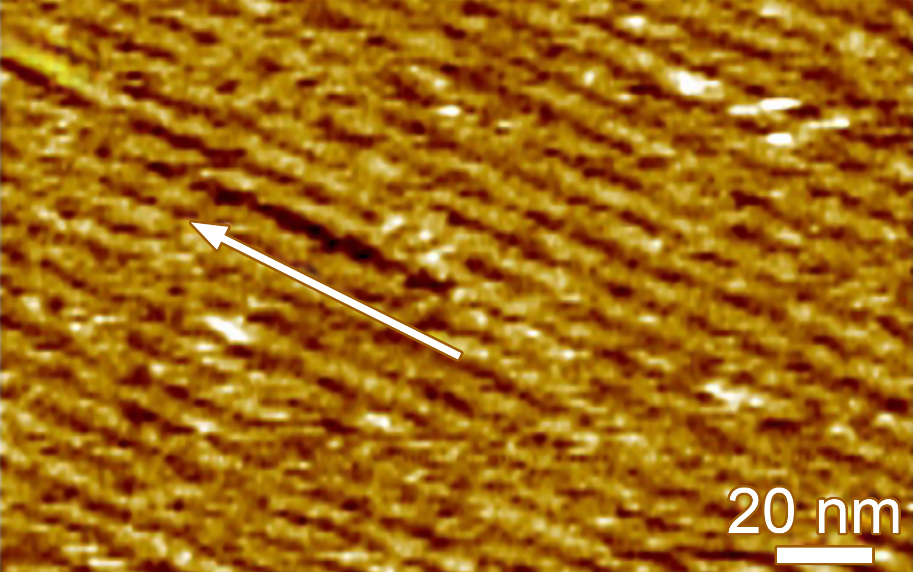
Now, a research team led by scientists at the Department of Energy’s Pacific Northwest National Laboratory has tamed the tangle. They report in the journal Science Advances that they have achieved a uniform two-dimensional (2D) layer of silk protein fragments, or “fibroins,” on graphene, a carbon-based material useful for its excellent electrical conductivity.
“These results provide a reproducible method for silk protein self-assembly that is essential for designing and fabricating silk-based electronics,” said Chenyang Shi, the study’s lead author. “It’s important to note that this system is nontoxic and water-based, which is crucial for biocompatibility.”
This combination of materials—silk-on-graphene—could form a sensitive, tunable transistor highly desired by the microelectronics industry for wearable and implantable health sensors. The PNNL team also sees potential for their use as a key component of memory transistors or “memristors,” in computing neural networks. Memristors, used in neural networks, allow computers to mimic how the human brain functions.
The Silk Road
For centuries, silkworm silk production was a closely guarded secret in China, while its fame spread through the celebrated Silk Road trade routes to India, the Middle East, and eventually Europe. By the Middle Ages, silk had become a status symbol and a coveted commodity in European markets. Even today, silk is associated with luxury and status.
The same underlying properties that make silk fabric world-renowned—elasticity, durability, and strength—have led to its use in advanced materials applications.
“There’s been a lot of research using silk as a way of modulating electronic signals, but because silk proteins are naturally disordered, there’s only so much control that’s been possible,” said James De Yoreo, a Battelle Fellow at PNNL with a dual appointment as a Professor of Materials Science and Engineering and of Chemistry at the University of Washington. “So, with our experience in controlling material growth on surfaces, we thought ‘what if we can make a better interface?’”
To do that, the team carefully controlled the reaction conditions, adding individual silk fibers to the water-based system in a precise manner. Through precision laboratory conditions, the team achieved a highly organized 2D layer of proteins packed in precise parallel β-sheets, one of the most common protein shapes in nature. Further imaging studies and complementary theoretical calculations showed that the thin silk layer adopts a stable structure with features found in natural silk. An electronic structure at this scale—less than half the thickness of a strand of DNA—supports the miniaturization found everywhere in the bio-electronics industry.
“This type of material lends itself to what we call field effects,” said De Yoreo. “This means that it’s a transistor switch that flips on or off in response to a signal. If you add, say, an antibody to it, then when a target protein binds, you cause a transistor to switch states.”
Indeed, the researchers are planning to use this starting material and technique to create their own artificial silk with functional proteins added to it to enhance its usefulness and specificity.
This study represents the first step in controlled silk layering on functional electronic components. Key areas of future research include improving the stability and conductivity of silk-integrated circuits and exploring silk’s potential in biodegradable electronics to increase the use of green chemistry in electronic manufacturing.